

What Role Does Boron Nitride Powder Play in the Production of Next Generation Semiconductors
2026-03-13
As the semiconductor industry pushes toward greater miniaturization and higher power densities, thermal management has become a critical challenge. Engineers and material scientists are increasingly turning to advanced materials to solve these problems. Among these, Boron Nitride Powder has emerged as a crucial component in the fabrication of next generation semiconductors, and Nextgen Advanced Materials is at the forefront of supplying this high-performance solution.
The Unique Properties of Boron Nitride Powder
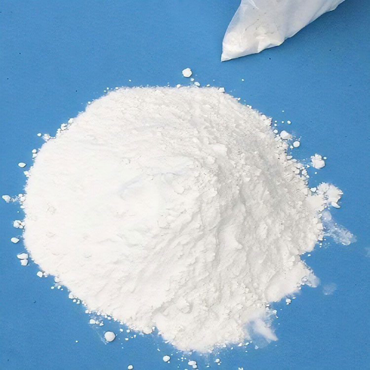
To understand its role in semiconductor production, it is essential to first examine the properties that make Boron Nitride Powder so valuable. Often referred to as "white graphite," it offers a combination of characteristics that are unmatched by traditional materials.
| Property | Benefit for Semiconductors |
|---|---|
| High Thermal Conductivity | Efficiently dissipates heat from sensitive components |
| Excellent Electrical Insulation | Prevents short circuits in densely packed devices |
| Chemical Inertness | Does not react with other materials during fabrication |
| High Temperature Stability | Performs reliably in deposition and annealing processes |
Critical Applications in Semiconductor Manufacturing
Nextgen Advanced Materials supplies Boron Nitride Powder that is utilized in several key areas of semiconductor production. Its versatility makes it indispensable for creating the high-performance chips required for modern electronics.
1. Thermal Interface Materials
As transistors shrink, heat density increases. Boron Nitride Powder is incorporated into thermal interface materials (TIMs) that are placed between the silicon die and the heat sink. Its high thermal conductivity ensures rapid heat transfer, which improves device performance and longevity.
2. Encapsulation and Molding Compounds
To protect delicate circuitry, semiconductors are encased in epoxy molding compounds. Adding Boron Nitride Powder to these compounds significantly enhances their ability to conduct heat away from the chip, without compromising their electrical insulating properties.
3. Substrates for Wide Bandgap Semiconductors
The production of next generation semiconductors made from materials like silicon carbide and gallium nitride often requires specialized substrates. Boron Nitride Powder is used in the creation of pyrolytic boron nitride (pBN) crucibles and heaters, which are essential for growing the high-purity crystals used in these devices.
Why Choose Boron Nitride Over Other Fillers?
While other ceramic fillers exist, Boron Nitride Powder offers distinct advantages that align perfectly with the demands of next generation semiconductors.
-
Superior Thermal Performance: It provides higher thermal conductivity than alumina or silica.
-
Dielectric Strength: It maintains excellent insulation even at very high voltages.
-
Particle Morphology: The platelet structure of hexagonal Boron Nitride Powder allows for better packing and thermal pathway formation in composites.
Boron Nitride Powder FAQ
What makes Boron Nitride Powder suitable for high-frequency semiconductor applications?
Boron Nitride Powder possesses a low dielectric constant and low dielectric loss tangent. In high-frequency applications, such as 5G and 6G communications, signal integrity is paramount. Materials that interfere with electrical signals can cause inefficiency and heat. Because Boron Nitride Powder is both thermally conductive and electrically insulating with minimal signal interference, it is the ideal filler for substrates and encapsulants used in high-speed, next generation semiconductor devices.
How does the purity of Boron Nitride Powder affect semiconductor manufacturing?
Purity is absolutely critical in semiconductor fabrication. Contaminants can migrate into the silicon lattice and alter the electrical properties of the device, leading to failure. Nextgen Advanced Materials ensures that its Boron Nitride Powder is processed to achieve extremely high purity levels. This minimizes the risk of introducing metal ions or other impurities into the clean manufacturing environment, ensuring higher yields and more reliable chips.
Can Boron Nitride Powder be used in the photolithography process?
While Boron Nitride Powder itself is not used directly in the photoresist or etching steps, it plays a vital role in the equipment that performs these processes. It is used to manufacture specialized ceramic components within the plasma etchers and deposition chambers. These components must withstand aggressive chemical plasmas and high temperatures without generating particulate contamination. The inert nature of Boron Nitride Powder makes it perfect for these critical machine parts, ensuring the precise conditions needed for nanometer-scale lithography are maintained.
The Future of Semiconductors with Advanced Materials
As the industry moves toward 3D chip stacking and heterogeneous integration, the need for materials that can manage heat in tight spaces will only grow. Boron Nitride Powder will continue to be a key enabler of these technologies. Nextgen Advanced Materials is dedicated to researching and developing new grades of this material to meet the evolving needs of semiconductor engineers.
Contact Us for Expert Solutions
Selecting the right material grade is critical for success in semiconductor applications. If you are developing next generation devices and require high-performance Boron Nitride Powder, our team is ready to assist you. Contact Nextgen Advanced Materials today to discuss your specific requirements and discover how our solutions can optimize your manufacturing process.